日益嚴格的環境法規繼續推動對半導體工廠用水有效管理的需求。
By Prakash Govindan, COO of Gradiant
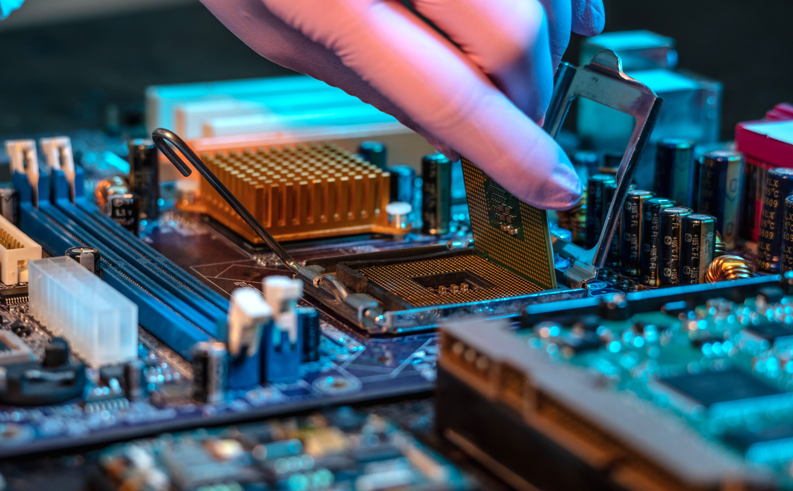
There is urgent need today for sustainability in water management at wafer fabrication and semiconductor manufacturing plants (or “fabs”). We are experiencing a global shortage of semiconductors that are required to control everything from automobiles to smartphones to appliances. As the semiconductor shortage persists, manufacturers are facing increasingly greater pressure to adopt sustainable and efficient practices in their water operations. Water serves a critical role in chip production, as it’s needed to rinse and clean silicon wafers as they are manufactured – and not just any water, but Ultrapure Water (UPW), which is thousands of times purer than drinking water. It takes roughly 1,400 -1,600 gallons of municipal water to make 1,000 gallons of UPW, with fabs using up to 5 million gallons daily.
At this time of unprecedented demand for semiconductors, severe droughts in major semiconductor manufacturing areas are threatening the operational continuity and expansion plans of brand owners and foundries. The intensive water consumption required by semiconductor fabs limits water availability for local households, businesses, and wildlife in the community. Further, in the major areas where fabs are located, such as Taiwan and the Western U.S., recent droughts have plagued these regions, thereby threatening the global supply chain, increasing the costs of production, and placing pressure on overall water availability.
水資源短缺的加劇影響新的技術趨勢
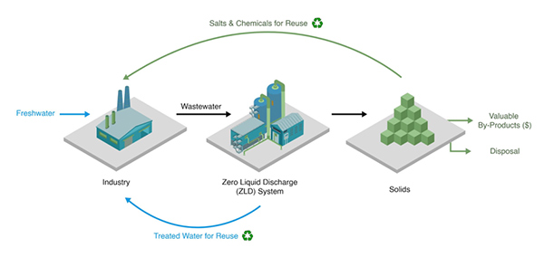
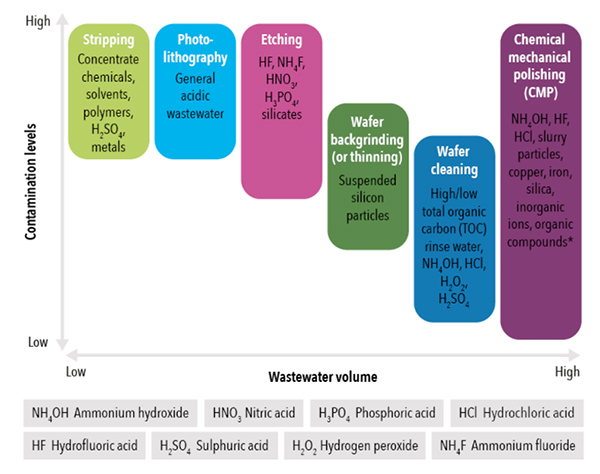
為了應對長期乾旱和對半導體不斷增長的需求,品牌所有者和製造商正在關注回收、減少和再利用生產中用水的新方法。水處理領域的新進展使半導體製造商能夠回收和再利用廢水、去除目標污染物,甚至從廢物流中回收有價值的產品。
由於易於實施,透過設備冷卻等簡單措施進行水回用繼續被廣泛採用,但工廠越來越有興趣處理和引導製程廢水的各個流,以作為超純水系統的給水。這種做法很複雜,因為每種廢水流都不同,有時需要自己的處理方法。當與其他水資源管理策略配合實施時,製造商可以大幅減少整體用水量,並確保其製造營運和供應鏈的可持續性和連續性。
來自世界領導人的壓力
Global leaders are becoming increasingly strict on water and wastewater quality and quantity as our freshwater resources are dwindling. Officials have recently announced ambitious goals to achieve a sustainable future, with a key focus to address the need for water. At the UN Climate Change Conference, better known as COP26, water was a primary focus of discussion. UN officials forecasted the world will see a 40% shortfall in water by 2030, prompting many leading brand owners from the world’s essential industries to pledge their operations will be net-water positive.
Outside of brand owners, many countries are also adopting initiatives for sustainable water management. In Asia, where most of the semiconductor manufacturing takes place, Singapore announced its Green Plan 2030 this year, to maximize the use of natural resources and reduce the amount of waste being discharged into the environment. As these initiatives and programs continue to grow and regulations related to water and wastewater management are enacted, brand owners and manufacturers are facing greater pressure to optimize their operations and minimize footprint through sustainable water practices.
未來的擴張計劃
未來對半導體的需求只會成長,以滿足我們日常生活中對科技和電子設備永不滿足的需求。水處理領域的創新進步現在使各行業能夠回收和再利用廢水、去除污染物並從廢物流中回收有價值的產品。隨著大型晶片工廠在未來幾年準備擴建,先進的水和廢水處理將在滿足世界對半導體的需求方面發揮關鍵作用。
日益嚴格的環境法規繼續推動對半導體工廠用水有效管理的需求。
By Prakash Govindan, COO of Gradiant
There is urgent need today for sustainability in water management at wafer fabrication and semiconductor manufacturing plants (or “fabs”). We are experiencing a global shortage of semiconductors that are required to control everything from automobiles to smartphones to appliances. As the semiconductor shortage persists, manufacturers are facing increasingly greater pressure to adopt sustainable and efficient practices in their water operations. Water serves a critical role in chip production, as it’s needed to rinse and clean silicon wafers as they are manufactured – and not just any water, but Ultrapure Water (UPW), which is thousands of times purer than drinking water. It takes roughly 1,400 -1,600 gallons of municipal water to make 1,000 gallons of UPW, with fabs using up to 5 million gallons daily.
At this time of unprecedented demand for semiconductors, severe droughts in major semiconductor manufacturing areas are threatening the operational continuity and expansion plans of brand owners and foundries. The intensive water consumption required by semiconductor fabs limits water availability for local households, businesses, and wildlife in the community. Further, in the major areas where fabs are located, such as Taiwan and the Western U.S., recent droughts have plagued these regions, thereby threatening the global supply chain, increasing the costs of production, and placing pressure on overall water availability.
水資源短缺的加劇影響新的技術趨勢
為了應對長期乾旱和對半導體不斷增長的需求,品牌所有者和製造商正在關注回收、減少和再利用生產中用水的新方法。水處理領域的新進展使半導體製造商能夠回收和再利用廢水、去除目標污染物,甚至從廢物流中回收有價值的產品。
由於易於實施,透過設備冷卻等簡單措施進行水回用繼續被廣泛採用,但工廠越來越有興趣處理和引導製程廢水的各個流,以作為超純水系統的給水。這種做法很複雜,因為每種廢水流都不同,有時需要自己的處理方法。當與其他水資源管理策略配合實施時,製造商可以大幅減少整體用水量,並確保其製造營運和供應鏈的可持續性和連續性。
來自世界領導人的壓力
Global leaders are becoming increasingly strict on water and wastewater quality and quantity as our freshwater resources are dwindling. Officials have recently announced ambitious goals to achieve a sustainable future, with a key focus to address the need for water. At the UN Climate Change Conference, better known as COP26, water was a primary focus of discussion. UN officials forecasted the world will see a 40% shortfall in water by 2030, prompting many leading brand owners from the world’s essential industries to pledge their operations will be net-water positive.
Outside of brand owners, many countries are also adopting initiatives for sustainable water management. In Asia, where most of the semiconductor manufacturing takes place, Singapore announced its Green Plan 2030 this year, to maximize the use of natural resources and reduce the amount of waste being discharged into the environment. As these initiatives and programs continue to grow and regulations related to water and wastewater management are enacted, brand owners and manufacturers are facing greater pressure to optimize their operations and minimize footprint through sustainable water practices.
未來的擴張計劃
未來對半導體的需求只會成長,以滿足我們日常生活中對科技和電子設備永不滿足的需求。水處理領域的創新進步現在使各行業能夠回收和再利用廢水、去除污染物並從廢物流中回收有價值的產品。隨著大型晶片工廠在未來幾年準備擴建,先進的水和廢水處理將在滿足世界對半導體的需求方面發揮關鍵作用。