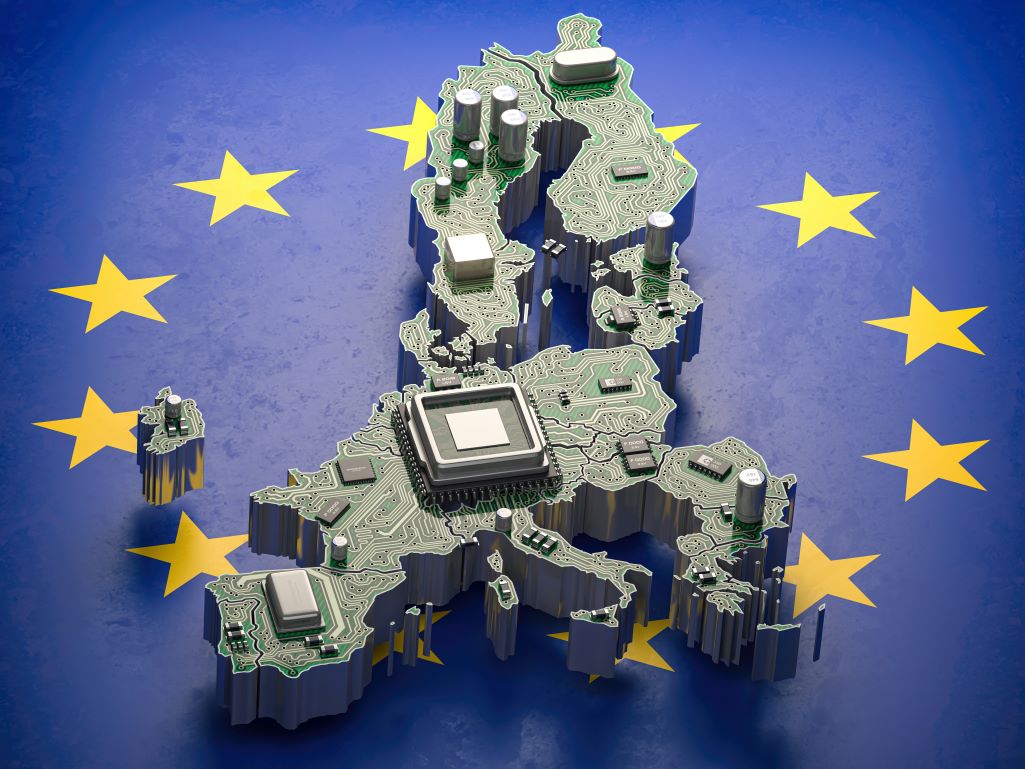
Europe is scaling up regional supply chain capabilities in semiconductor manufacturing, with Germany taking the lead. Minimizing the water footprint through innovations in water reuse, MLD/ZLD and AI/ML digital solutions have become top of mind in the design and operation of new fabs in the region. Global Water Intelligence (GWI) met with Gradiant’s H+E Group to discuss the crucial role of water recycling in reducing consumption and the surging growth of semiconductor manufacturing in the region as the European Chips Act takes hold.
GERMANY – December 21, 2023 – As Germany’s semiconductor industry springs to life in the wake of new EU development rules aimed at improving local production capacity, Europe is starting to seriously consider its options for the industry – and its stringent water requirements.
While the ultrapure water (UPW) demands of the sector are slightly less extreme than in other regions, the focus on water reuse and minimising consumption offers serious potential for high-value treatment schemes to be implemented.
Activity in Germany has focused around hotspots like Dresden, where the Taiwan Semiconductor Manufacturing Company (TSMC) is planning to locate a new facility – joining Bosch, X-Fab, and the expanding Infineon plants. This led to the announcement this year of the Dresden Drainage Board’s €600 million “Dresden 600” project. This will see the capacity of the Dresden-Kaditz wastewater treatment plant increase by 100,000 p.e. to prepare for the growing volumes of industrial wastewater from the semiconductor sector, as well as to meet increasingly stringent EU regulatory standards. The contract for the WWTP expansion is currently out to tender, with bids expected in February 2024.
While plants prepare for additional influent to municipal sewers, there is interest from the industry in reducing discharges and maximising water recycling on-site. “With rising water scarcity in places like Germany, the fabs can’t rely on the local municipality’s drinking water as a source, so they’re having to seek alternate sources,” Daniel Bewg, business development director at H+E, told GWI. “They need a larger water treatment system, and they want to recycle as much of that water as possible.”
This follows a global trend towards ambitious sustainability targets from semiconductor companies, improving the outlook for water efficiency and reuse projects. In the case of Global Foundries, its Dresden fab faces more water stress than its Singapore or USA locations. This led its Dresden “Fab 1” to install a UPW recycling plant with a 75% recovery rate to reduce water consumption by 300,000m3 per year, as well as several water conservation projects that save an estimated 30,000m3 of UPW annually.
Change in UPW Demand
Though the larger chip sizes currently produced in Europe have slightly simpler water requirements then the smallest chips driving the American and Asian markets, UPW quality demands are rising as more advanced fabs pop up in the region.
This comes as EU politicians and the industrial sector look to gain some autonomy from global chip supply chains. “What Europe is lacking is manufacturing facilities for chips that require the smallest node size that exists,” explained Frank Bösenberg, managing director of semiconductor industry organisation Silicon Saxony. “If you go smaller than 10 nanometres, no one in Europe at the moment is able to manufacture those – this is where the Intel investment is supposed to help.”
While Intel’s planned Magdeburg facility is expected to produce the smallest chips in Europe, the water requirements at other advanced facilities, such as the upcoming TSMC facility which will produce 12nm chips, still represent significant opportunities for UPW providers. Considering that chip demand in Europe is driven strongly by the typically larger chip nodes of the automotive industry, it is unlikely there will be a complete shift towards the smallest node sizes. Even so, a notable shift towards more advanced nodes and bigger fabs is driving the sector’s water needs forward.
Europe Acts
The European Chips Act, which entered into force in September 2023, provides a framework to allow member states to subsidise the semiconductor industry. Germany has been the most active in utilising this act to mobilise funding, with €20 billion made available to support companies locating or expanding manufacturing plants there. This successfully drew plans for fabs from Intel, Infineon, ZF/Wolfspeed, and TSMC – amounting to planned investments in manufacturing of €48 billion. With such large facilities planned, substantial water contracts are expected to follow.
The initial success seen in Germany has yet to be replicated elsewhere in Europe at scale, however. Other than funding from Germany and the EU itself (€11.15 billion by 2030), only Spain has committed to subsidising the industry (€12.25 billion by 2027). While individual projects and expansions have been outlined in Spain, France, Poland, and the Czech Republic, attracting the semiconductor industry could prove challenging without further hefty subsidy programmes. This makes the lofty EU ambitions to capture a 20% share of the global semiconductor market by 2030 – from the current level of approximately 8% – look extremely ambitious.
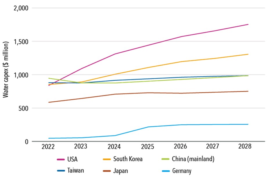
Hence, while interest is rising from key players in the UPW sector and a slew of growth has occurred, it will likely take a significant increase in long-term government support programmes to meet these ambitions. Nonetheless, with the global microelectronics sector set to almost double by 2030, the burgeoning water-related capex in the sector is still expected to grow at a CAGR of 36.5% in Germany between 2023 and 2028, and by 7.9% in Western Europe as a whole.
Which Micro-Markets will spend most on Water?
Germany is the leading light for Europe’s semiconductor industry, and spending on related water treatment facilities is set to rise rapidly as a result.
H+E’s Bewg emphasised that the supply chain must react appropriately to growth. “Water quality demands are typically higher in America and Asia, but in Europe it’s starting to go towards that level. Companies are coming into Europe and bringing with them higher water quality demands, which means that your supply chain is getting squeezed quite a bit at the moment, because we’re not used to seeing this level of activity in Europe.”
Supply chain opportunities
While much of the anticipated water activity is still in the planning stages, UPW suppliers are preparing to secure footholds in the burgeoning European market. This has been shown in a spate of UPW acquisitions announced in the space of this year alone: Gradiant’s acquisition of Aquarion AG (parent company of H+E), Kurita’s acquisition of turnkey UPW plant provider Arcade Engineering Group, and Exyte acquiring high-purity water systems supplier Intega.
Having a strong physical presence on the continent is crucial to ensuring effective service delivery in the sector. For companies already established in the region, such as UPW market leader Ovivo, the focus is instead on expanding its offering. Philippe Rychen, global director of innovation at Ovivo, told us: “We are strongly active in innovation, mainly due to the fact that we want to serve our customers, so we have to provide them with top-quality solutions.”
Along with the necessary technical offerings for producing UPW, Bewg highlighted that the scale of projects creates additional requirements from the semiconductor industry. “They want somebody who’s got proven experience and is able to execute these larger projects, so financial stability is also something they look for.”